Guidelines
Good schematics show you the circuit. Bad schematics make you decipher them. Here you can find a bunch of guidelines we set up to get consistent schematics along the project.
Schematics
Clean Text placement
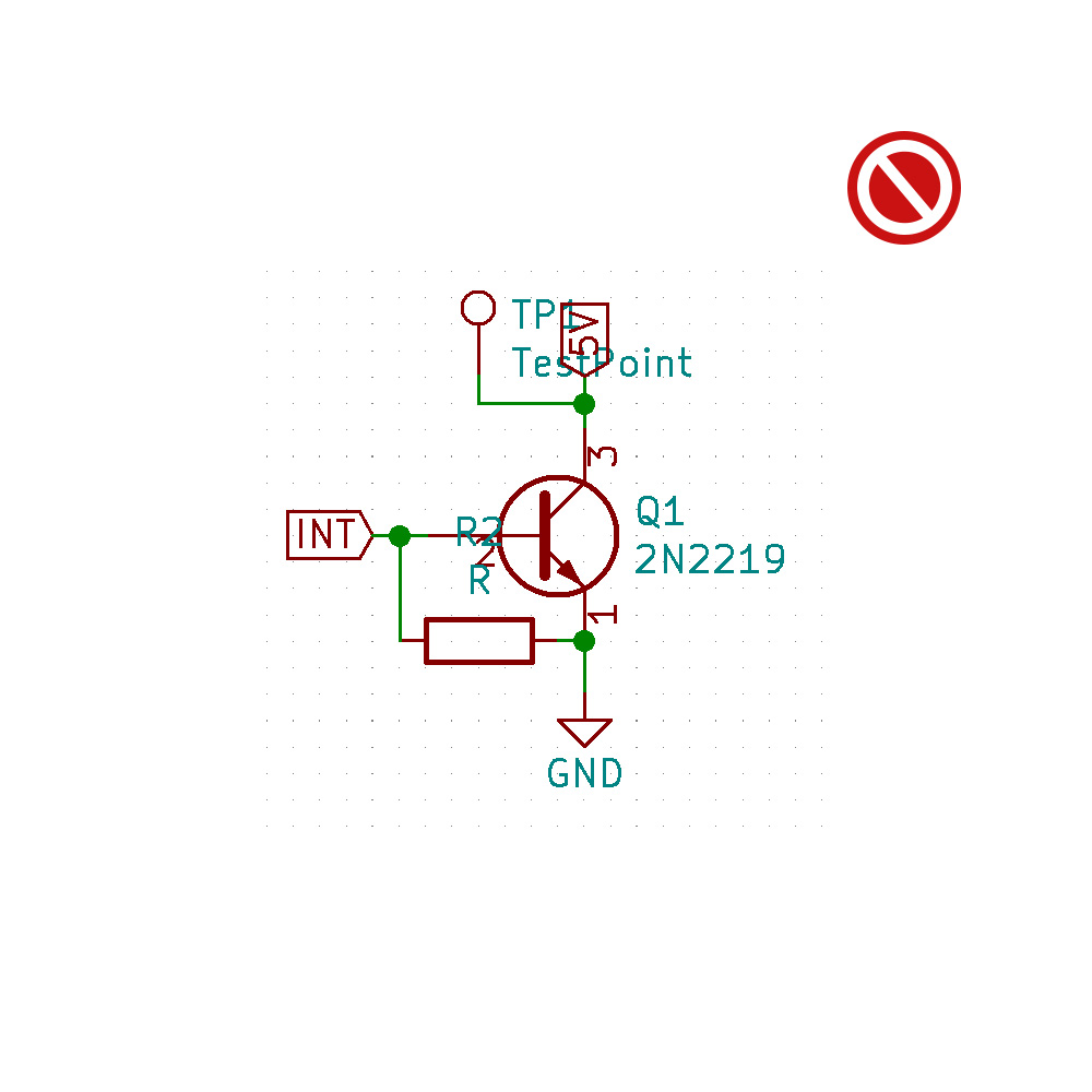
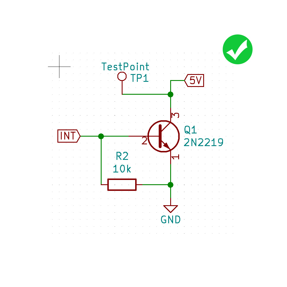
After placing a symbol make sure the designator is close to the symbol and does not overlap other text or tracks
Make some space and move parts if they are too close
Do not place text verticaly
Layout flow
Logical flow from left to right
Power connectioncs should go up to positive voltages and down to negative voltages
Rotate common symbols the same way to find similarities faster in a schematics
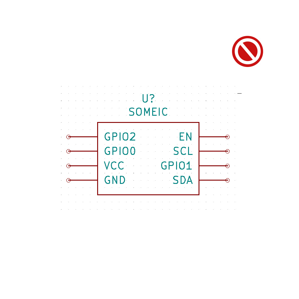
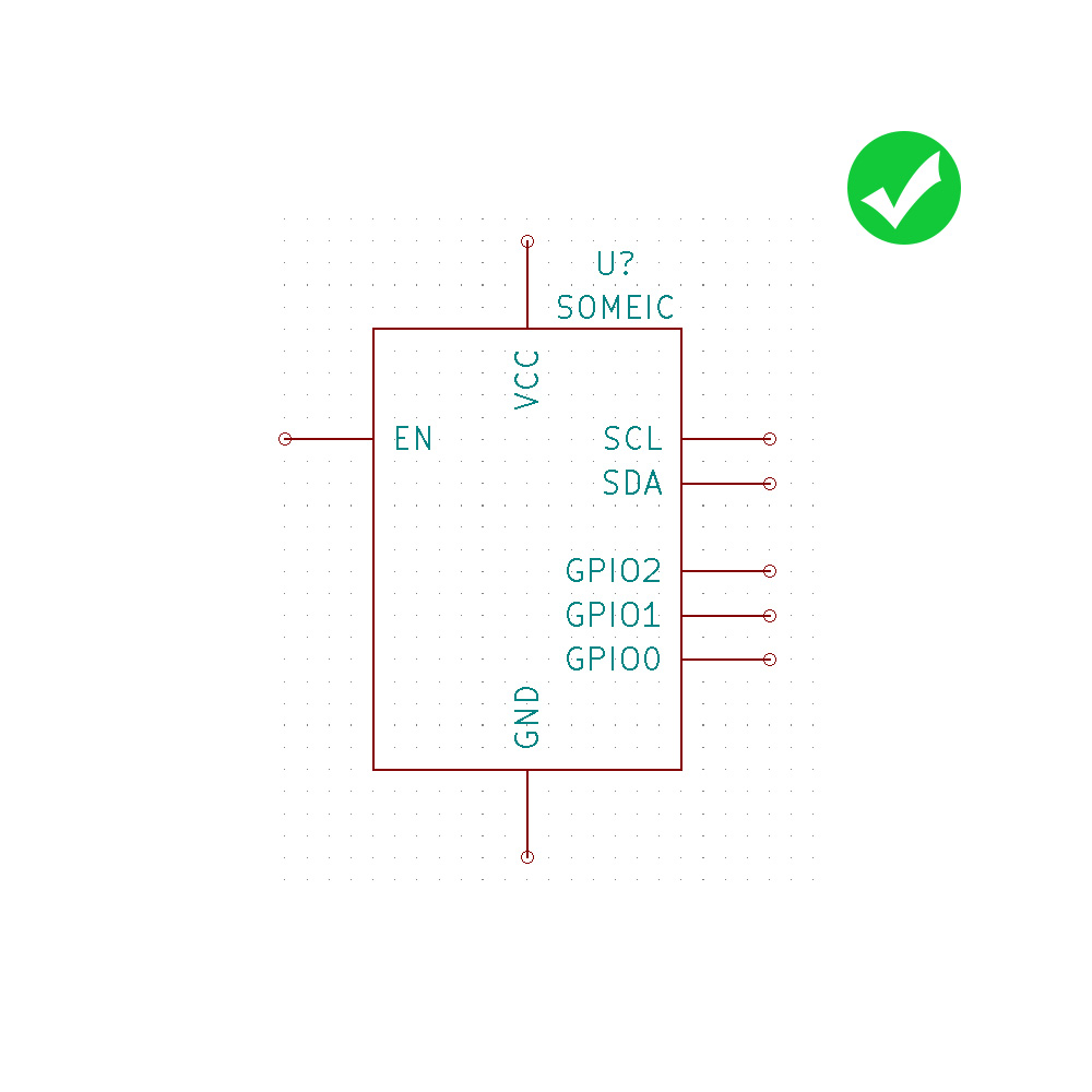
Schematic Symbols
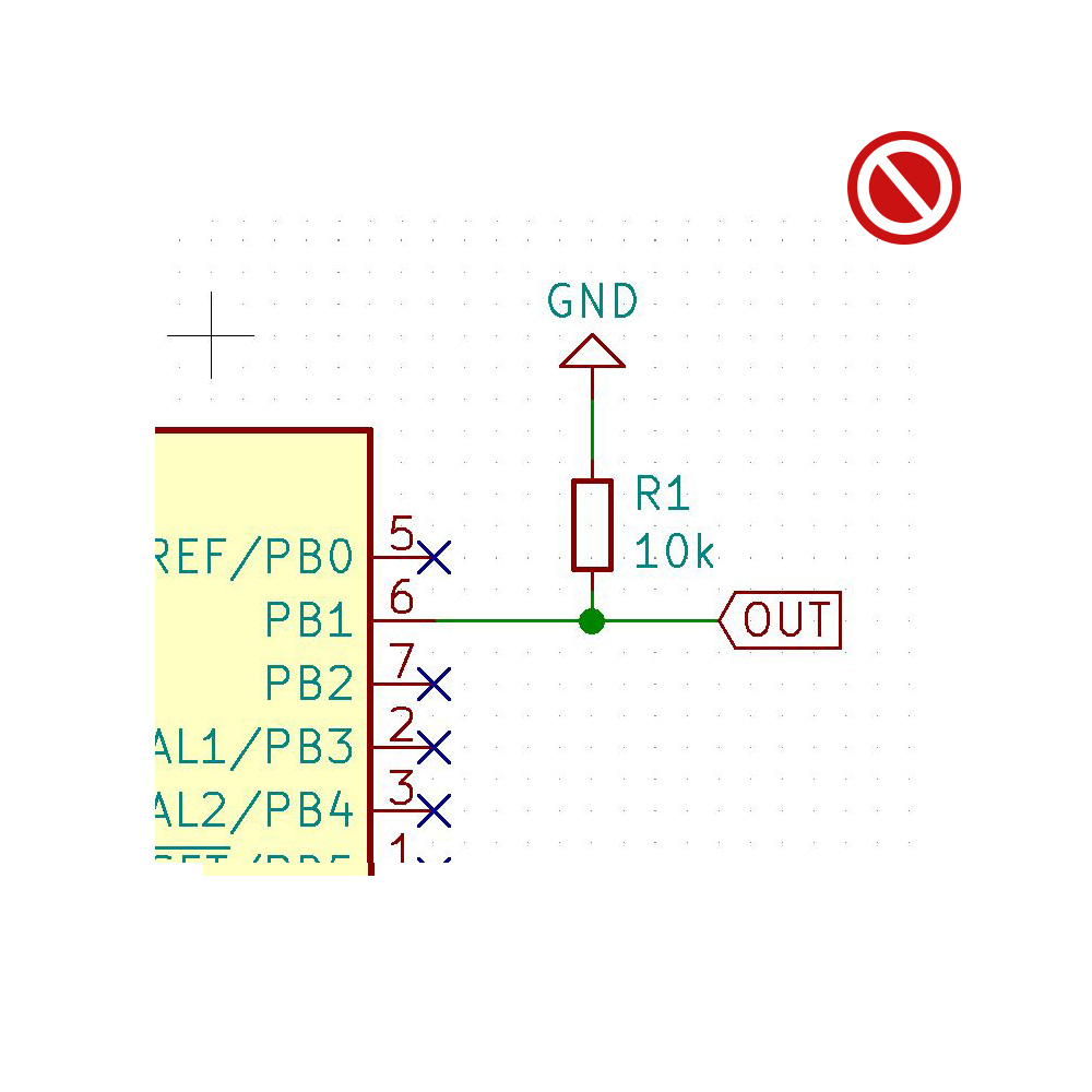
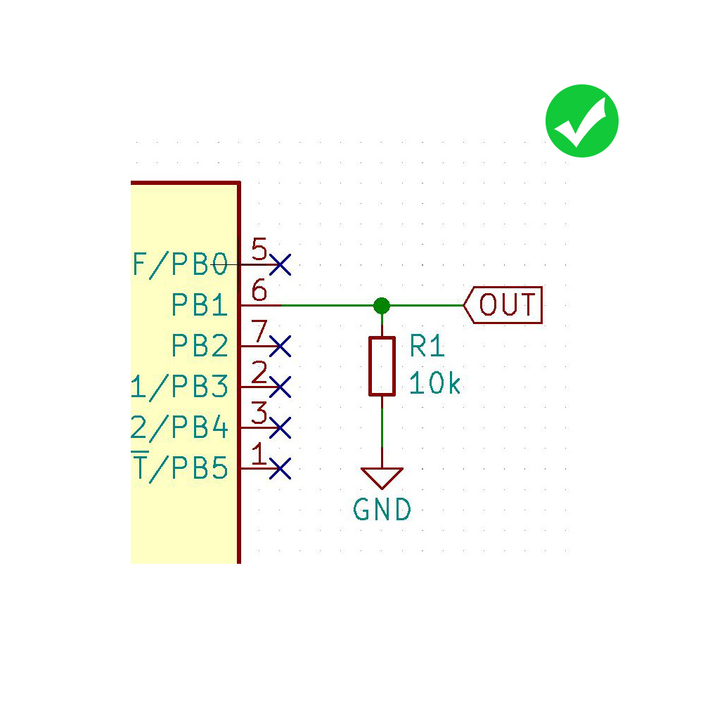
Show pins of an IC in a position relevant to their function, not how they happen to stick out of the chip.
Positive pins top the top
Negative pins to the bottom
Inputs to the left
Outputs to the right
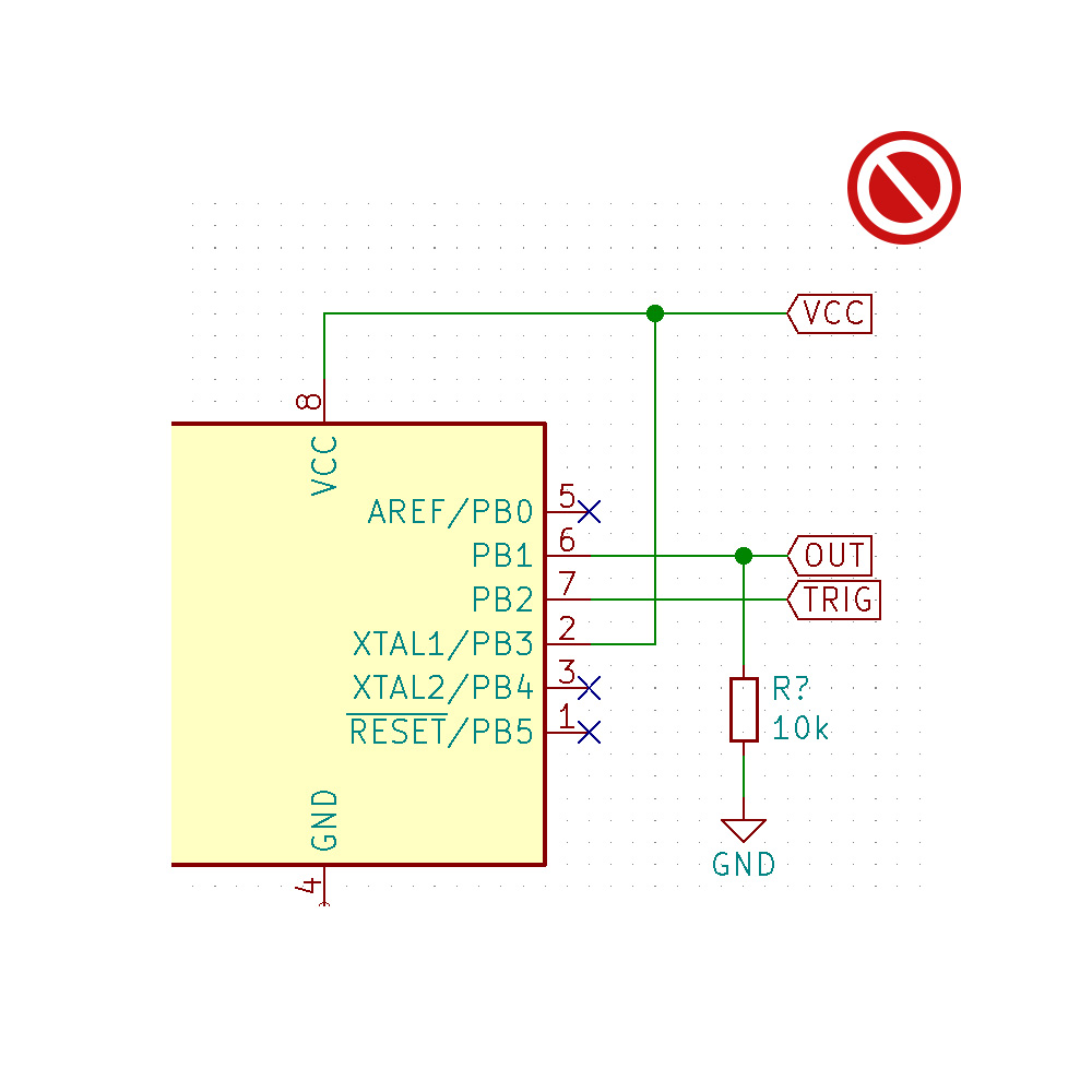
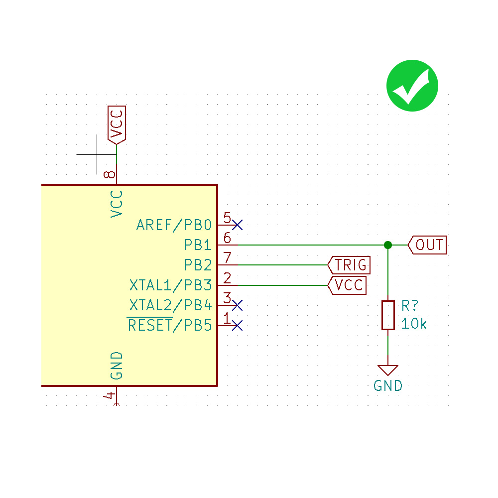
Direct connections, within reason
reduce wire crossing and alike as much as possible for clarity
draw dots on junctions if your tool does not do it for you (if not you should use a better one)
NETs and Labels
Give your NETs nicely readable names
But keep them reasonably short
Always try to use your tool to select a NET instead of writing it by hand to avoind spelling mistakes
Use upper case for NET Labels
See this ANSI/IEEE standard for recommended pin name abbreviations.